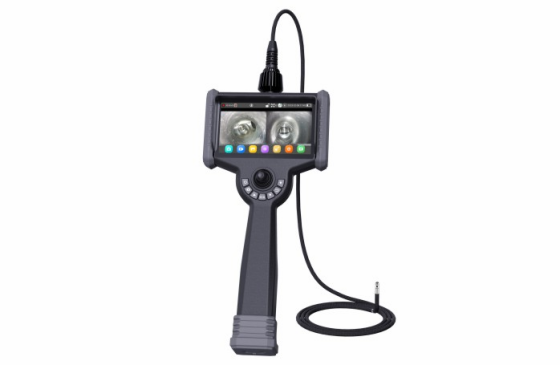
Application of industrial endoscopes in the electronics manufacturing industry
The application of industrial endoscopes in the electronics manufacturing field has deeply penetrated the entire process of R&D, production and maintenance, becoming a core tool for ensuring product quality and efficiency. Its non-destructive detection characteristics and high-precision imaging capabilities provide the following key support for the electronics manufacturing industry:
Semiconductor and Chip Manufacturing Quality Control
In semiconductor manufacturing, industrial endoscopes use ultra-fine probes (diameter <0.5mm) to penetrate chip packages and inspect for solder joint defects, wafer impurities, and misalignment between layers. For example, in advanced packaging processes, endoscopes can observe the quality of through-hole interconnects in 3D stacked chips in real time. Combined with 3D measurement technology, they can quantify defects such as pits and cracks to ensure process yield. A semiconductor manufacturer used endoscopes to detect internal impurities in wafers, increasing yield by 12% and reducing inspection cycle time by 40%.
Precision Inspection of Consumer Electronics Assembly
In the assembly of consumer electronics products such as smartphones and tablets, endoscopes are used to detect problems such as shorts/opens in through-holes within multi-layer circuit boards and poor solder joints in BGAs. For example, flexible probes (bend radius ≤2mm) can penetrate deep into camera modules or battery connectors to verify sealing and solder integrity. A mobile phone manufacturer used endoscopes to inspect internal motherboard circuitry, reducing failure rates by 25% and reducing rework costs. 3. Electronic Equipment Fault Diagnosis and Maintenance
Industrial endoscopes play a vital role in the maintenance of complex electronic systems, such as servers and industrial control equipment. For example, they can detect corrosion on server motherboards or loose hard drive connectors to prevent downtime. Using AI image recognition technology to automatically identify short circuits on circuit boards, one data center has reduced repair time by 70%. Furthermore, endoscopes can be used for non-contact inspection in extreme environments, such as nuclear power plant control equipment and spacecraft electronic modules.
Process Optimization and R&D Support
During the development phase of electronics manufacturing, endoscopes provide real-time observation of micron-level defects in key processes like photolithography and etching, assisting engineers in optimizing process parameters. For example, high-definition imaging (up to 4K resolution) can be used to identify etching residues and adjust process times to improve uniformity. A research institute uses endoscopes combined with thermal imaging to analyze stress distribution in power device packages, providing data support for material selection.
Technological Evolution and Industry Trends
Currently, industrial endoscopes are evolving towards ultra-fineness and intelligence. Nanoscale probes (0.1mm diameter) have entered the laboratory stage, enabling inspection of even tinier electronic components. AI algorithms automatically classify solder defects through deep learning, achieving a 98% detection accuracy rate. Furthermore, 5G technology enables real-time cloud storage of inspection data, building equipment health profiles and supporting predictive maintenance. These innovations are further driving electronics manufacturing toward zero defects, reducing overall costs while improving product reliability.


